KASAN ELECTRONICS CO., LTD.
WINX
|
Category |
Video |
|
Video Types Supported |
XVGA |
|
Video Processor |
Tseng Labs ET-4000/32P |
|
Highest Resolution Supported |
1280 x 1024 |
|
Data Bus Type |
32-bit PCI |
|
Memory Type |
DRAM |
|
Maximum Onboard Memory |
2MB |
|
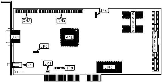
CONNECTIONS | |||
|
Purpose |
Location |
Purpose |
Location |
|
15-pin analog video port |
CN1 |
Imagne port connector |
CN3 |
|
Feature connector |
CN2 |
3D jack |
J1 |
|
INTERRUPT CONFIGURATION | ||
|
IRQ 2/9 |
JP1 | |
| » |
Enabled |
Open |
|
Disabled |
Closed | |
|
PCI ID DETECTION CONFIGURATION | ||
|
Setting |
JP3 | |
| » |
Detected at start up |
Pins 1 & 2 closed |
|
Detected by ROM BIOS |
Pins 2 & 3 closed | |
|
MEMORY CLOCK CONFIGURATION | ||
|
Setting |
JP4 | |
| » |
50MHz |
Pins 1 & 2 closed |
|
44.7MHz |
Pins 2 & 3 closed | |
|
BASE I/O ADDRESS SELECTION | ||
|
Address |
JP5 | |
| » |
258h, 259h |
Pins 2 & 3 closed |
|
358h, 359h |
Pins 1 & 2 closed | |
|
DRAM CONFIGURATION | ||
|
Size |
Bank 0 |
Bank 1 |
|
1MB |
(2) 256K x 16 |
NONE |
|
2MB |
(2) 256K x 16 |
(2) 256K x 16 |
|
MISCELLANEOUS TECHNICAL NOTE |
|
The exact location of pin 1 on JP3, JP4 & JP5 is unidentified by the manufacturer. |