UNIDENTIFIED
LX400A/G
|
Processor |
80486SX/80487SX/80486DX/80486DX2 |
|
Processor Speed |
25/33/40/50(internal)/50/66(internal) MHz |
|
Chip Set |
SiS |
|
Max. Onboard DRAM |
32MB |
|
Cache |
64/128/256 |
|
BIOS |
AMI |
|
Dimensions |
230mm x 218mm |
|
I/O Options |
32-bit VESA local bus slots (2), PS/2 mouse port |
|
NPU Options |
None |
|
CONNECTIONS | |||
|
Purpose |
Location |
Purpose |
Location |
|
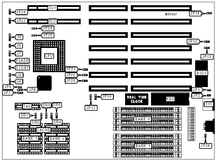
Flash LED connector |
FLASH |
Power LED & keylock |
J7 |
|
Turbo LED |
J3 |
PS/2 mouse connector |
J11 |
|
Turbo switch |
J4 |
Standby output connector |
J28 |
|
Speaker |
J5 |
32-bit VESA Local bus slot |
S1 |
|
Reset switch |
J6 |
32-bit VESA Local bus slot |
S2 |
|
USER CONFIGURABLE SETTINGS | |||
|
Function |
Jumper |
Position | |
|
» |
Factory configured do not alter |
JP1 |
Open |
|
» |
Monitor type select color |
JP2 |
Closed |
|
Monitor type select monochrome |
JP2 |
Open | |
|
» |
Factory configured do not alter |
JP10 |
N/A |
|
» |
Factory configured do not alter |
JP11 |
N/A |
|
PS/2 mouse interrupt |
JP12 |
pins 1 & 2 closed | |
|
PS/2 mouse set at AT Bus IRQ12 |
JP12 |
pins 2 & 3 closed | |
|
» |
Factory configured do not alter |
JP13 |
N/A |
|
» |
Factory configured do not alter |
JP14 |
N/A |
|
» |
Factory configured do not alter |
JP21 |
N/A |
|
» |
Factory configured do not alter |
JP22 |
N/A |
|
» |
Factory configured do not alter |
JP23 |
N/A |
|
» |
Power saving mode switch off |
STDBY |
Open |
|
Power saving mode switch on |
STDBY |
Closed | |
|
DRAM CONFIGURATION | ||
|
Size |
Bank 0 |
Bank 1 |
|
1MB |
(4) 256K x 9 |
NONE |
|
2MB |
(4) 256K x 9 |
(4) 256K x 9 |
|
4MB |
(4) 1M x 9 |
NONE |
|
8MB |
(4) 1M x 9 |
(4) 1M x 9 |
|
16MB |
(4) 4MB x 9 |
(4) 4MB x 9 |
|
20MB |
(4) 1MB x9 |
(4) 4MB x 9 |
|
32MB |
(4) 4MB x 9 |
(4) 4MB x 9 |
|
CACHE JUMPER CONFIGURATION | |||||
|
Size |
SR1 |
SR2 |
SR3 |
SR4 |
SR5 |
|
64KB |
pins 2 & 3 |
pins 2 & 3 |
pins 1 & 2 |
pins 1 & 2 |
pins 1 & 2 |
|
128KB |
pins 1 & 2 |
pins 1 & 2 |
pins 2 & 3 |
pins 2 & 3 |
pins 1 & 2 |
|
256KB |
pins 2 & 3 |
pins 2 & 3 |
pins 2 & 3 |
pins 2 & 3 |
pins 2 & 3 |
|
Note:Pins designated are in the closed position. | |||||
|
CACHE CONFIGURATION | |||
|
Size |
Bank 0 |
Bank 1 |
TAG |
|
64 KB |
(4) 8K x 8 |
(4) 8K x 8 |
(1) 8K x 8 |
|
128 KB |
(4) 32K x 8 |
NONE |
(1) 8K x 8 |
|
256 KB |
(4) 32K x 8 |
(4) 32K x 8 |
(1) 32K x 8 |
|
CPU TYPE CONFIGURATION | |||
|
CPU Type |
JP6 |
JP7 |
JP8 |
|
80486SX |
Open |
Open |
pins 2 & 3 closed |
|
80487SX |
Closed |
pins 2 & 3 closed |
pins 1 & 2 closed |
|
80486DX |
Closed |
pins 1 & 2 closed |
pins 1 & 2 closed |
|
CPU SPEED CONFIGURATION | |||
|
CPU speed |
S0 |
S1 |
S2 |
|
25 MHz |
Closed |
Open |
Open |
|
33 MHz |
Closed |
Closed |
Closed |
|
40 MHz |
Closed |
Closed |
Closed |
|
50 MHz |
Open |
Open |
Closed |
|
50iMHz |
Closed |
Open |
Open |
|
60iMHz |
Closed |
Closed |
Closed |
|
Note:The location on the system board of the above jumpers is unidentified. | |||
|
VESA WAIT STATE/BUS SPEED CONFIGURATION | |||
|
CPU Speed |
Wait states |
JP24, JP26 |
JP25, JP27 |
|
< 33MHz |
0 wait states |
pins 1 & 2 closed |
pins 1 & 2 closed |
|
> 33MHz |
1 wait state |
pins 2 & 3 closed |
pins 2 & 3 closed |
|
MISCELLANEOUS TECHNICAL NOTE |
|
Note:Some of the SR jumpers may be hard-wired by the manufacturer, thus some of the cache options may not be available. |