UNIDENTIFIED
MB286T 20
|
Processor |
80286 |
|
Processor Speed |
20MHz |
|
Chip Set |
Goldstar |
|
Max. Onboard DRAM |
5MB |
|
Cache |
None |
|
BIOS |
AMI |
|
Dimensions |
220mm x 230mm |
|
I/O Options |
None |
|
NPU Options |
80287 |
|
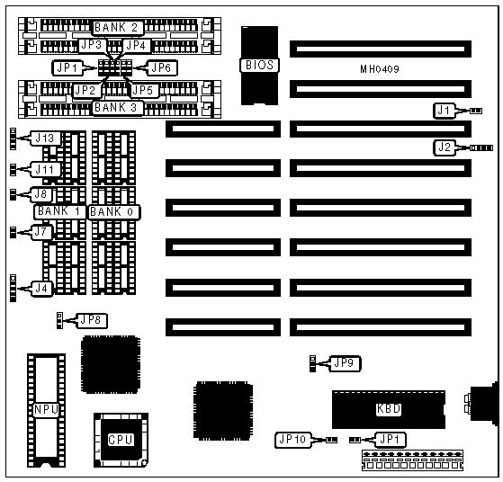
CONNECTIONS |
|||
|
Purpose |
Location |
Purpose |
Location |
|
Power LED & keylock |
J4 |
Turbo LED |
J8 |
|
External battery |
J2 |
Reset switch |
J11 |
|
Turbo switch |
J7 |
Speaker |
J13 |
|
USER CONFIGURABLE SETTINGS |
|||
|
Function |
Jumper |
Position |
|
|
» |
CMOS memory normal operation |
J1 |
Closed |
|
|
CMOS memory clear |
J1 |
Open |
|
» |
Factory configured - do not alter |
JP1 |
N/A |
|
» |
Factory configured - do not alter |
JP8 |
N/A |
|
» |
Factory configured - do not alter |
JP9 |
N/A |
|
» |
Monitor type select color |
JP10 |
Closed |
|
|
Monitor type select monochrome |
JP10 |
Open |
|
DRAM CONFIGURATION |
||||||
|
Size |
Bank 0 |
Parity 0 |
Bank 1 |
Parity 1 |
Bank 2 |
Bank 3 |
|
512KB |
(4) 44256 |
(2) 41256 |
NONE |
NONE |
NONE |
NONE |
|
1MB |
(4) 44256 |
(2) 41256 |
(4) 44256 |
(2) 41256 |
NONE |
NONE |
|
2MB |
(4) 44256 |
(2) 41256 |
(4) 44256 |
(2) 41256 |
(2) 256K x 9 |
(2) 256K x 9 |
|
3MB |
(4) 44256 |
(2) 41256 |
(4) 44256 |
(2) 41256 |
(2) 1M x 9 |
NONE |
|
5MB |
(4) 44256 |
(2) 41256 |
(4) 44256 |
(2) 41256 |
(2) 1M x 9 |
(2) 1M x 9 |
|
Note: This table for use when banks 0 & 1 are used for base memory and banks 2 & 3 are used for expansion memory. |
||||||
|
DRAM CONFIGURATION |
||||
|
Size |
Bank 0 |
Bank 1 |
Bank 2 |
Bank 3 |
|
512KB |
NONE |
NONE |
(2) 256K x 9 |
NONE |
|
1MB |
NONE |
NONE |
(2) 256K x 9 |
(2) 256K x 9 |
|
2MB |
NONE |
NONE |
(2) 1M x 9 |
NONE |
|
2.5MB |
NONE |
NONE |
(2) 256K x 9 |
(2) 1M x 9 |
|
4MB |
NONE |
NONE |
(2) 1M x 9 |
(2) 1M x 9 |
|
Note: This table for use when banks 2 & 3 are used for base memory only. |
||||
|
BASE MEMORY CONFIGURATION |
|
|
Banks |
JP1, JP2, JP3, JP4, JP5 & JP6 |
|
Base memory : Banks 2 & 3 |
pins 1 & 2 closed |
|
Base memory : Banks 0 & 1 (Expansion memory : Banks 2 & 3) |
pins 2 & 3 closed |
|
Note: Exact arrangement & size of DIPP sockets unidentified. |
|