TYAN COMPUTER CORPORATION
S1696DLUA
|
Device Type |
Mainboard |
|
Processor |
Pentium II |
|
Processor Speed |
200/233/266/300/333MHz |
|
Chip Set |
Intel |
|
Video Chip Set |
None |
|
Maximum Onboard Memory |
1GB (EDO & SDRAM supported) |
|
Maximum Video Memory |
None |
|
Cache |
256/512KB (located on Pentium II CPU) |
|
BIOS |
AMI |
|
Dimensions |
305mm x 244mm |
|
I/O Options |
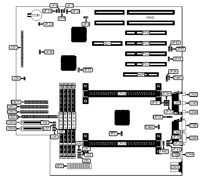
32-bit PCI slots (4), floppy drive interface, game port, green PC connector, IDE interfaces (2), SCSI interface, Wide Ultra SCSI interface, parallel port, PS/2 mouse port, serial ports (2), IR connector, USB connectors (2), ATX power connector, AGP slot, line in, line out, microphone in, RAID slot |
|
NPU Options |
None |
|
CONNECTIONS | |||
|
Purpose |
Location |
Purpose |
Location |
|
AGP slot |
AGP |
Ultra Wide SCSI interface |
CN15 |
|
ATX power connector |
ATX |
Ultra Wide SCSI interface |
CN16 |
|
Game port |
CN1 |
Chassis fan power |
FAN1 |
|
Microphone in |
CN2 |
Chassis fan power |
FAN2 |
|
Line in |
CN3 |
Chassis fan power |
FAN3 |
|
Line out |
CN4 |
Soft off power supply |
J25/pins 1 & 2 |
|
Serial port 2 |
CN5 |
Green PC connector |
J25/pins 3 & 4 |
|
Serial port 1 |
CN6 |
IR connector |
J25/pins 6 - 11 |
|
Parallel port |
CN7 |
IDE interface LED |
J25/pins 13 - 16 |
|
USB connector 1 |
CN8 |
Power LED |
J25/pins 18 - 20 |
|
USB connector 2 |
CN9 |
Reset switch |
J25/pins 22 & 23 |
|
PS/2 mouse port |
CN10 |
Speaker |
J25/pins 24 - 27 |
|
Floppy drive interface |
CN11 |
Wake on LAN connector |
JP21 |
|
IDE interface 1 |
CN12 |
SCSI interface LED |
JP22 |
|
IDE interface 2 |
CN13 |
32-bit PCI slots |
PC1 – PC4 |
|
SCSI interface |
CN14 |
RAID slot |
SL1 |
|
USER CONFIGURABLE SETTINGS | |||
|
Function |
Label |
Position | |
|
» |
Factory configured - do not alter |
J20 |
Unidentified |
|
» |
Factory configured - do not alter |
JP2 |
Open |
|
» |
CMOS memory normal operation |
JP3 |
Pins 1 & 2 closed |
|
CMOS memory clear |
JP3 |
Pins 2 & 3 closed | |
|
» |
Flash BIOS voltage select 5v |
JP4 |
Pins 1 & 2 closed |
|
Flash BIOS voltage select 12v |
JP4 |
Pins 2 & 3 closed | |
|
» |
SCSI PCI ID select AD 26 |
JP23 |
Pins 1 & 2 closed |
|
SCSI PCI ID select AD 24 |
JP23 |
Pins 2 & 3 closed | |
|
» |
Factory configured - do not alter |
JP30A |
Unidentified |
|
» |
Factory configured - do not alter |
JP31 |
Unidentified |
|
» |
Factory configured - do not alter |
JP32 |
Unidentified |
|
» |
Factory configured - do not alter |
JP33 |
Unidentified |
|
» |
Factory configured - do not alter |
JP34 |
Unidentified |
|
» |
Factory configured - do not alter |
JP36 |
Unidentified |
|
» |
Factory configured - do not alter |
JP38 |
Closed |
|
USER CONFIGURABLE SETTINGS (CON’T) | |||
|
Function |
Label |
Position | |
|
» |
Factory configured - do not alter |
JP39 |
Closed |
|
» |
Factory configured - do not alter |
JP40 |
Open |
|
» |
Factory configured - do not alter |
JP48 |
Open |
|
Note: The location of JP48 is unidentified. | |||
|
DIMM CONFIGURATION | ||||
|
Size |
Bank 0 |
Bank 1 |
Bank 2 |
Bank 3 |
|
8MB |
(1) 1M x 64 |
None |
None |
None |
|
16MB |
(1) 2M x 64 |
None |
None |
None |
|
16MB |
(1) 1M x 64 |
(1) 1M x 64 |
None |
None |
|
24MB |
(1) 2M x 64 |
(1) 1M x 64 |
None |
None |
|
24MB |
(1) 1M x 64 |
(1) 1M x 64 |
(1) 1M x 64 |
None |
|
32MB |
(1) 4M x 64 |
None |
None |
None |
|
32MB |
(1) 2M x 64 |
(1) 2M x 64 |
None |
None |
|
32MB |
(1) 1M x 64 |
(1) 1M x 64 |
(1) 1M x 64 |
(1) 1M x 64 |
|
40MB |
(1) 4M x 64 |
(1) 1M x 64 |
None |
None |
|
48MB |
(1) 4M x 64 |
(1) 2M x 64 |
None |
None |
|
48MB |
(1) 2M x 64 |
(1) 2M x 64 |
(1) 2M x 64 |
None |
|
64MB |
(1) 2M x 64 |
(1) 2M x 64 |
(1) 2M x 64 |
(1) 2M x 64 |
|
64MB |
(1) 8M x 64 |
None |
None |
None |
|
64MB |
(1) 4M x 64 |
(1) 4M x 64 |
None |
None |
|
72MB |
(1) 8M x 64 |
(1) 1M x 64 |
None |
None |
|
80MB |
(1) 8M x 64 |
(1) 2M x 64 |
None |
None |
|
96MB |
(1) 8M x 64 |
(1) 4M x 64 |
None |
None |
|
96MB |
(1) 4M x 64 |
(1) 4M x 64 |
(1) 4M x 64 |
None |
|
128MB |
(1) 16M x 64 |
None |
None |
None |
|
128MB |
(1) 8M x 64 |
(1) 8M x 64 |
None |
None |
|
128MB |
(1) 4M x 64 |
(1) 4M x 64 |
(1) 4M x 64 |
(1) 4M x 64 |
|
136MB |
(1) 16M x 64 |
(1) 1M x 64 |
None |
None |
|
144MB |
(1) 16M x 64 |
(1) 2M x 64 |
None |
None |
|
152MB |
(1) 16M x 64 |
(1) 1M x 64 |
(1) 1M x 64 |
(1) 1M x 64 |
|
160MB |
(1) 16M x 64 |
(1) 4M x 64 |
None |
None |
|
176MB |
(1) 16M x 64 |
(1) 2M x 64 |
(1) 2M x 64 |
(1) 2M x 64 |
|
192MB |
(1) 16M x 64 |
(1) 8M x 64 |
None |
None |
|
DIMM CONFIGURATION (CON’T) | ||||
|
Size |
Bank 0 |
Bank 1 |
Bank 2 |
Bank 3 |
|
192MB |
(1) 8M x 64 |
(1) 8M x 64 |
(1) 8M x 64 |
None |
|
224MB |
(1) 16M x 64 |
(1) 4M x 64 |
(1) 4M x 64 |
(1) 4M x 64 |
|
256MB |
(1) 32M x 64 |
None |
None |
None |
|
256MB |
(1) 16M x 64 |
(1) 16M x 64 |
None |
None |
|
256MB |
(1) 8M x 64 |
(1) 8M x 64 |
(1) 8M x 64 |
(1) 8M x 64 |
|
272MB |
(1) 16M x 64 |
(1) 16M x 64 |
(1) 1M x 64 |
(1) 1M x 64 |
|
280MB |
(1) 32M x 64 |
(1) 1M x 64 |
(1) 1M x 64 |
(1) 1M x 64 |
|
288MB |
(1) 16M x 64 |
(1) 16M x 64 |
(1) 2M x 64 |
(1) 2M x 64 |
|
304MB |
(1) 32M x 64 |
(1) 2M x 64 |
(1) 2M x 64 |
(1) 2M x 64 |
|
320MB |
(1) 16M x 64 |
(1) 16M x 64 |
(1) 4M x 64 |
(1) 4M x 64 |
|
320MB |
(1) 16M x 64 |
(1) 8M x 64 |
(1) 8M x 64 |
(1) 8M x 64 |
|
352MB |
(1) 32M x 64 |
(1) 4M x 64 |
(1) 4M x 64 |
(1) 4M x 64 |
|
384MB |
(1) 16M x 64 |
(1) 16M x 64 |
(1) 16M x 64 |
None |
|
448MB |
(1) 32M x 64 |
(1) 8M x 64 |
(1) 8M x 64 |
(1) 8M x 64 |
|
512MB |
(1) 32M x 64 |
(1) 32M x 64 |
None |
None |
|
512MB |
(1) 16M x 64 |
(1) 16M x 64 |
(1) 16M x 64 |
(1) 16M x 64 |
|
640MB |
(1) 32M x 64 |
(1) 16M x 64 |
(1) 16M x 64 |
(1) 16M x 64 |
|
768MB |
(1) 32M x 64 |
(1) 32M x 64 |
(1) 32M x 64 |
None |
|
1024MB |
(1) 32M x 64 |
(1) 32M x 64 |
(1) 32M x 64 |
(1) 32M x 64 |
|
Note: Board accepts EDO & SDRAM memory. Maximum SDRAM is 512MB. Maximum EDO is 1GB. | ||||
|
DIMM VOLTAGE CONFIGURATION | |||||
|
Voltage |
J30 |
J31 |
J32 |
J33 | |
| » |
3.3v |
Closed |
Closed |
Closed |
Closed |
|
5v |
Open |
Open |
Open |
Open | |
|
DIMM VOLTAGE CONFIGURATION (CON’T) | |||||
|
Voltage |
J34 |
J35 |
J36 |
J37 | |
| » |
3.3v |
Open |
Open |
Open |
Open |
|
5v |
Closed |
Closed |
Closed |
Closed | |
|
CACHE CONFIGURATION |
|
Note: 256KB/512KB cache is located on the Pentium II CPU. |
|
CPU SPEED SELECTION | ||||||
|
CPU speed |
Clock speed |
Multiplier |
JP7 |
JP8 |
JP9 |
JP10 |
|
200MHz |
66MHz |
3x |
Closed |
Closed |
Open |
Closed |
|
233MHz |
66MHz |
3.5x |
Closed |
Open |
Open |
Closed |
|
266MHz |
66MHz |
4x |
Closed |
Closed |
Closed |
Open |
|
300MHz |
66MHz |
4.5x |
Closed |
Open |
Closed |
Open |
|
333MHz |
66MHz |
5x |
Closed |
Closed |
Open |
Open |
|
SERIAL PORT SELECTION | ||||
|
Setting |
JP41 |
JP42 |
JP45 |
JP46 |
|
Used as serial port |
Pins 1 & 2 closed |
Pins 1 & 2 closed |
Closed |
Open |
|
Used as IR connector |
Pins 2 & 3 closed |
Pins 2 & 3 closed |
Open |
Closed |
|
Note: The location of JP45 & JP46 is unidentified. | ||||
|
SCSI TERMINATION SELECTION | |||
|
Setting |
JP43 |
JP44 | |
| » |
SCSI high byte enabled |
Pins 1 & 2 closed |
Pins 1 & 2 closed |
|
Controlled by SCSI chip |
Pins 2 & 3 closed |
Pins 2 & 3 closed | |