TYAN COMPUTER CORPORATION
S1468
|
Processor |
Pentium |
|
Processor Speed |
75/90/100/120/133/150/166MHz |
|
Chip Set |
Intel |
|
Max. Onboard DRAM |
128MB |
|
Cache |
256/512KB |
|
BIOS |
AMI/Award |
|
Dimensions |
330mm x 218mm |
|
I/O Options |
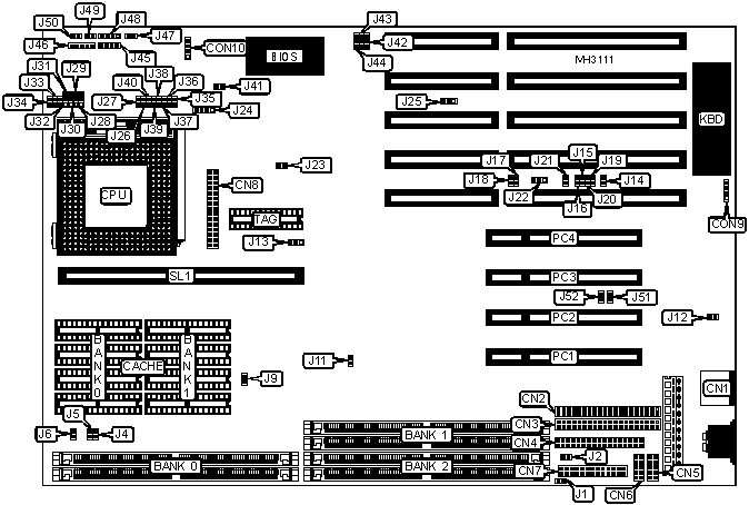
32-bit PCI slots (4), floppy drive interface, IDE interfaces (2), parallel port, PS/2 mouse port, serial ports (2), cache slot, Infra Red connectors (2), VRM connector |
|
NPU Options |
None |
|
CONNECTIONS | |||
|
Purpose |
Location |
Purpose |
Location |
|
PS/2 mouse port |
CN1 |
Infra Red interface |
CON10 |
|
IDE interface 2 |
CN2 |
Speaker |
J45 |
|
IDE interface 1 |
CN3 |
Power LED & keylock |
J46 |
|
Floppy drive interface |
CN4 |
Turbo switch |
J47 |
|
Serial port 1 |
CN5 |
IDE interface LED |
J48 pins 1 & 2 |
|
Serial port 2 |
CN6 |
Reset switch |
J49 |
|
Parallel port |
CN7 |
Turbo LED |
J50 |
|
VRM connector |
CN8 |
32-bit PCI slots |
PC1 - PC4 |
|
Infra Red interface |
CON9 |
Cache slot |
SL1 |
|
USER CONFIGURABLE SETTINGS | |||
|
Function |
Jumper |
Position | |
|
» |
Factory configured - do not alter |
J12 |
N/A |
|
» |
Factory configured - do not alter |
J14 |
N/A |
|
» |
Factory configured - do not alter |
J15 |
N/A |
|
» |
Factory configured - do not alter |
J16 |
N/A |
|
» |
Factory configured - do not alter |
J17 |
N/A |
|
» |
Factory configured - do not alter |
J18 |
N/A |
|
» |
Factory configured - do not alter |
J19 |
N/A |
|
» |
Factory configured - do not alter |
J20 |
N/A |
|
» |
Factory configured - do not alter |
J21 |
N/A |
|
» |
Factory configured - do not alter |
J22 |
pins 2 & 3 closed |
|
» |
Factory configured - do not alter |
J23 |
N/A |
|
Chipset type select SMC 665IR (set at factory do not alter) |
J25 |
pins 1 & 2 closed | |
|
Chipset type select SMC 669IR (set at factory do not alter) |
J25 |
pins 2 & 3 closed | |
|
» |
Factory configured - do not alter |
J26 |
Closed |
|
» |
Factory configured - do not alter |
J27 |
Closed |
|
» |
Factory configured - do not alter |
J34 |
N/A |
|
» |
Factory configured - do not alter |
J35 |
Open |
|
» |
Factory configured - do not alter |
J36 |
Closed |
|
» |
Factory configured - do not alter |
J37 |
Open |
|
» |
Factory configured - do not alter |
J38 |
Open |
|
» |
Factory configured - do not alter |
J39 |
Closed |
|
» |
Factory configured - do not alter |
J40 |
Open |
|
» |
CMOS memory normal operation |
J41 |
Open |
|
CMOS memory clear |
J41 |
Closed | |
|
» |
Factory configured - do not alter |
J42 |
pins 1 & 2 closed |
|
» |
Factory configured - do not alter |
J43 |
pins 1 & 2 closed |
|
» |
Factory configured - do not alter |
J44 |
pins 1 & 2 closed |
|
DRAM CONFIGURATION | |||
|
Size |
Bank 0 |
Bank 1 |
Bank 2 |
|
8MB |
(2) 1M x 32 |
NONE |
NONE |
|
32MB |
(2) 4M x 32 |
NONE |
NONE |
|
16MB |
(2) 1M x 32 |
(2) 1M x 32 |
NONE |
|
24MB |
(2) 1M x 32 |
(2) 1M x 32 |
(2) 1M x 32 |
|
32MB |
(2) 1M x 32 |
(2) 1M x 32 |
(2) 2M x 32 |
|
48MB |
(2) 1M x 32 |
(2) 1M x 32 |
(2) 4M x 32 |
|
80MB |
(2) 1M x 32 |
(2) 1M x 32 |
(2) 8M x 32 |
|
48MB |
(2) 4M x 32 |
(2) 2M x 32 |
NONE |
|
56MB |
(2) 4M x 32 |
(2) 2M x 32 |
(2) 1M x 32 |
|
64MB |
(2) 4M x 32 |
(2) 2M x 32 |
(2) 2M x 32 |
|
80MB |
(2) 4M x 32 |
(2) 2M x 32 |
(2) 4M x 32 |
|
112MB |
(2) 4M x 32 |
(2) 2M x 32 |
(2) 8M x 32 |
|
32MB |
NONE |
(2) 4M x 32 |
NONE |
|
40MB |
NONE |
(2) 4M x 32 |
(2) 1M x 32 |
|
48MB |
NONE |
(2) 4M x 32 |
(2) 2M x 32 |
|
64MB |
NONE |
(2) 4M x 32 |
(2) 4M x 32 |
|
96MB |
NONE |
(2) 4M x 32 |
(2) 8M x 32 |
|
64MB |
NONE |
(2) 8M x 32 |
NONE |
|
72MB |
NONE |
(2) 8M x 32 |
(2) 1M x 32 |
|
80MB |
NONE |
(2) 8M x 32 |
(2) 2M x 32 |
|
96MB |
NONE |
(2) 8M x 32 |
(2) 4M x 32 |
|
128MB |
NONE |
(2) 8M x 32 |
(2) 8M x 32 |
|
CACHE CONFIGURATION | ||||
|
Size |
Bank 0 |
Bank 1 |
TAG |
SL1 |
|
256KB (A) |
(4) 32K x 8 |
(4) 32K x 8 |
(1) 32K x 8 |
Not installed |
|
256KB (B) |
NONE |
NONE |
NONE |
Installed |
|
512KB (A) |
(4) 64K x 8 |
(4) 64K x 8 |
(1) 32K x 8 |
Not installed |
|
512KB (B) |
NONE |
NONE |
NONE |
Installed |
|
Note: If SL1 is used, Banks 0 & 1 and TAG must be removed. | ||||
|
CACHE JUMPER CONFIGURATION | |||||
|
Size |
J13 |
J28 |
J29 |
J30 |
J31 |
|
256KB |
2 & 3 |
1 & 2 |
2 & 3 |
2 & 3 |
1 & 2 |
|
512KB |
1 & 2 |
2 & 3 |
1 & 2 |
2 & 3 |
1 & 2 |
|
Cache module |
N/A |
1 & 2 |
1 & 2 |
1 & 2 |
1 & 2 |
|
Note: Pins designated should be in the closed position. | |||||
|
CPU SPEED CONFIGURATION | |||
|
Speed |
J24 |
J32 |
J33 |
|
75MHz |
pins 1 & 2, 3 & 4 closed |
Open |
Open |
|
90MHz |
pins 3 & 4 closed |
Open |
Open |
|
100MHz |
pins 1 & 2 closed |
Open |
Open |
|
120MHz |
pins 3 & 4 closed |
Closed |
Open |
|
133MHz |
pins 1 & 2 closed |
Closed |
Open |
|
150MHz |
pins 1 & 2, 3 & 4 closed |
Open |
Closed |
|
166MHz |
pins 1 & 2 closed |
Closed |
Closed |
|
CPU VOLTAGE CONFIGURATION | |||||||
|
Voltage |
J1 |
J2 |
J4 |
J5 |
J6 |
J9 |
J11 |
|
3.3v |
Open |
Open |
Closed |
Closed |
Closed |
Open |
Open |
|
5v |
Closed |
Closed |
Open |
Open |
Open |
Closed |
Closed |
|
INFRA RED CONFIGURATION | ||
|
Setting |
J51 |
J52 |
|
Normal I/O |
pins 1 & 2 closed |
pins 1 & 2 closed |
|
IR support |
pins 2 & 3 closed |
pins 2 & 3 closed |