TMC RESEARCH CORPORATION
JATO 286+
|
Processor |
80286 |
|
Processor Speed |
10/12/16/20MHz |
|
Chip Set |
LSI |
|
Max. Onboard DRAM |
8MB |
|
Cache |
None |
|
BIOS |
Unidentified |
|
Dimensions |
330mm x 218mm |
|
I/O Options |
None |
|
NPU Options |
80287 |
|
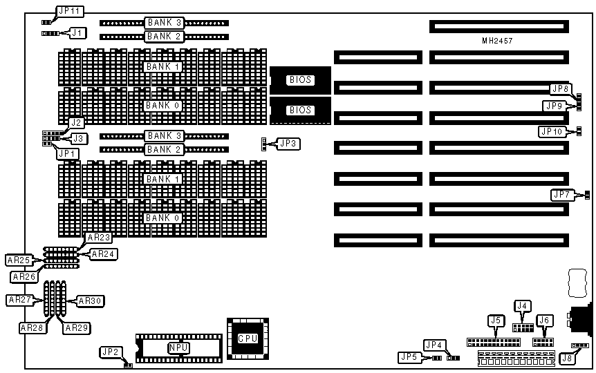
CONNECTIONS | |||
|
Purpose |
Location |
Purpose |
Location |
|
Turbo LED |
J1 |
Serial port 1 |
J6 |
|
Power LED & keylock |
J2 |
External battery |
J8 |
|
Speaker |
J3 |
Reset switch |
JP1 |
|
Serial port 2 |
J4 |
Reset switch |
JP5 |
|
Parallel port |
J5 | ||
|
USER CONFIGURABLE SETTINGS | |||
|
Function |
Jumper |
Position | |
|
» |
NPU clock speed select CPU clock |
JP2 |
pins 1 & 2 closed |
|
NPU clock speed select OSC1 |
JP2 |
pins 2 & 3 closed | |
|
» |
BIOS type select 27128 |
JP3 |
pins 1 & 2 closed |
|
BIOS type select 27256 |
JP3 |
pins 2 & 3 closed | |
|
» |
Power good signal detect from board |
JP4 |
pins 2 & 3 closed |
|
Power good signal detect from power supply |
JP4 |
pins 1 & 2 closed | |
|
» |
Monitor type select color |
JP6 |
Closed |
|
Monitor type select monochrome |
JP6 |
Open | |
|
» |
Battery type select internal |
JP7 |
Closed |
|
Battery type select external |
JP7 |
Open | |
|
» |
Parallel port enabled |
JP8 |
Open |
|
Parallel port disabled |
JP8 |
Closed | |
|
» |
Serial port 2 enabled |
JP9 |
Open |
|
Serial port 2 disabled |
JP9 |
Closed | |
|
» |
Serial port 1 enabled |
JP10 |
Open |
|
» |
Serial port 1 disabled |
JP10 |
Closed |
|
Factory configured - do not alter |
JP11 |
Open | |
|
Note: The location of JP6 is unidentified. | |||
|
DRAM CONFIGURATION (OPTION 1) | ||||
|
Size |
Bank 0 |
Bank 1 |
Bank 2 |
Bank 3 |
|
512KB |
(18) 41256 |
NONE |
NONE |
NONE |
|
640KB |
(18) 41256 |
(18) 4164 |
NONE |
NONE |
|
1MB |
(18) 41256 |
(18) 41256 |
NONE |
NONE |
|
2MB |
(18) 41256 |
(18) 41256 |
(2) 256K x 9 |
(2) 256K x 9 |
|
4MB |
(18) 411000 |
(18) 411000 |
NONE |
NONE |
|
5MB |
(18) 411000 |
(18) 411000 |
(2) 256K x 9 |
(2) 256K x 9 |
|
8MB |
(18) 411000 |
(18) 411000 |
(2) 1M x 9 |
(2) 1M x 9 |
|
DRAM CONFIGURATION (OPTION 2) | ||||
|
Size |
Bank 0 |
Bank 1 |
Bank 2 |
Bank 3 |
|
512KB |
NONE |
NONE |
(2) 256K x 9 |
NONE |
|
1MB |
NONE |
NONE |
(2) 256K x 9 |
(2) 256K x 9 |
|
2MB |
(18) 41256 |
(18) 41256 |
(2) 256K x 9 |
(2) 256K x 9 |
|
4MB |
NONE |
NONE |
(2) 1M x 9 |
(2) 1M x 9 |
|
5MB |
(18) 41256 |
(18) 41256 |
(2) 1M x 9 |
(2) 1M x 9 |
|
5MB |
(18) 411000 |
(18) 411000 |
(2) 256K x 9 |
(2) 256K x 9 |
|
8MB |
(18) 411000 |
(18) 411000 |
(2) 1M x 9 |
(2) 1M x 9 |
|
DRAM RESISTOR CONFIGURATION | ||||
|
Size |
AR23 |
AR24 |
AR25 |
AR26 |
|
Option 1 |
Installed |
Installed |
Not Installed |
Not Installed |
|
Option 2 |
Not Installed |
Not Installed |
Installed |
Installed |
|
DRAM RESISTOR CONFIGURATION (CON’T) | ||||
|
Size |
AR27 |
AR28 |
AR29 |
AR30 |
|
Option 1 |
Not Installed |
Not Installed |
Installed |
Installed |
|
Option 2 |
Installed |
Installed |
Not Installed |
Not Installed |