TMC RESEARCH CORPORATION
PAT3XCA
|
Processor |
80386SX |
|
Processor Speed |
16MHz |
|
Chip Set |
NEAT |
|
Max. Onboard DRAM |
8MB |
|
Cache |
None |
|
BIOS |
Unidentified |
|
Dimensions |
330mm x 215mm |
|
I/O Options |
None |
|
NPU Options |
80387SX |
|
CONNECTIONS | |||
|
Purpose |
Location |
Purpose |
Location |
|
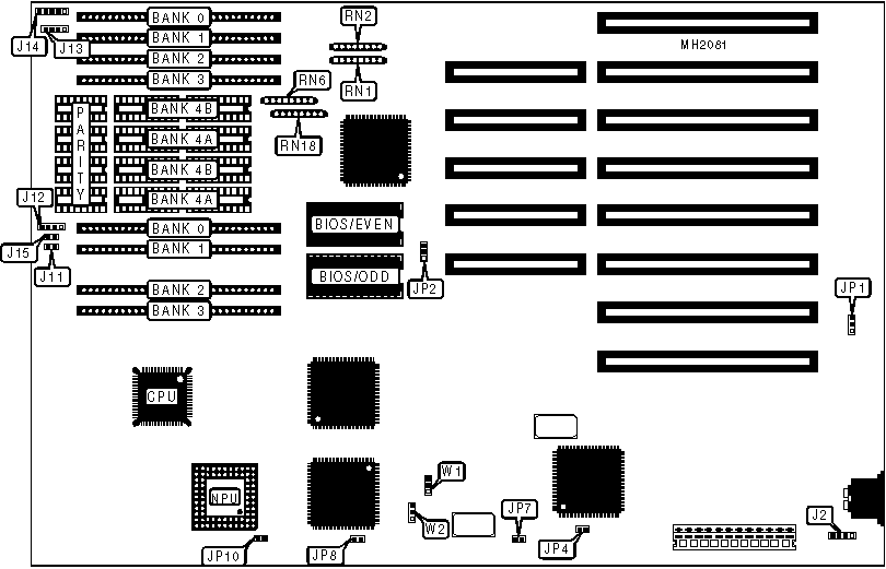
External battery |
J2 |
Speaker |
J13 |
|
Reset switch |
J11 |
Power LED & keylock |
J14 |
|
Turbo LED |
J12 |
Turbo switch |
J15 |
|
USER CONFIGURABLE SETTINGS | |||
|
Function |
Jumper |
Position | |
|
» |
Battery type select internal |
JP1 |
pins 1 & 2 closed |
|
Battery type select external |
JP1 |
Open | |
|
» |
BIOS type select 27256 |
JP2 |
pins 2 & 3 closed |
|
BIOS type select 27128 |
JP2 |
pins 1 & 2 closed | |
|
» |
Monitor type select color |
JP4 |
Closed |
|
Monitor type select monochrome |
JP4 |
Open | |
|
» |
NPU disabled |
JP7 |
Closed |
|
NPU enabled |
JP7 |
Open | |
|
» |
Pipeline mode enabled |
JP8 |
Closed |
|
Pipeline mode disabled |
JP8 |
Open | |
|
» |
Factory configured - do not alter |
JP10 |
N/A |
|
» |
Factory configured - do not alter |
W1 |
N/A |
|
» |
Factory configured - do not alter |
W2 |
N/A |
|
DRAM CONFIGURATION | |||||||
|
Size |
Bank 0 |
Bank 1 |
Bank 2 |
Bank 3 |
Bank 4A |
Bank 4B |
PARITY |
|
512KB |
(2) 256K x 9 |
NONE |
NONE |
NONE |
NONE |
NONE |
NONE |
|
512KB |
NONE |
NONE |
NONE |
NONE |
(4) 44256 |
NONE |
(2) 41256 |
|
1MB |
(2) 256K x 9 |
(2) 256K x 9 |
NONE |
NONE |
NONE |
NONE |
NONE |
|
1MB |
(2) 256K x 9 |
NONE |
NONE |
NONE |
(4) 44256 |
NONE |
(2) 41256 |
|
1MB |
NONE |
NONE |
(2) 256K x 9 |
NONE |
(4) 44256 |
NONE |
(2) 41256 |
|
1MB |
NONE |
NONE |
NONE |
NONE |
(4) 44256 |
(4) 44256 |
(4) 41256 |
|
2MB |
(2) 256K x 9 |
(2) 256K x 9 |
(2) 256K x 9 |
(2) 256K x 9 |
NONE |
NONE |
NONE |
|
2MB |
(2) 1M x 9 |
NONE |
NONE |
NONE |
NONE |
NONE |
NONE |
|
2MB |
(2) 256K x 9 |
(2) 256K x 9 |
NONE |
NONE |
(4) 44256 |
(4) 44256 |
(4) 41256 |
|
2MB |
NONE |
NONE |
(2) 256K x 9 |
(2) 256K x 9 |
(4) 44256 |
(4) 44256 |
(4) 41256 |
|
3MB |
(2) 1M x 9 |
NONE |
NONE |
NONE |
(4) 44256 |
(4) 44256 |
(4) 41256 |
|
3MB |
NONE |
NONE |
(2) 1M x 9 |
NONE |
(4) 44256 |
(4) 44256 |
(4) 41256 |
|
4MB |
(2) 1M x 9 |
(2) 1M x 9 |
NONE |
NONE |
NONE |
NONE |
NONE |
|
5MB |
(2) 256K x 9 |
(2) 256K x 9 |
(2) 1M x 9 |
(2) 1M x 9 |
NONE |
NONE |
NONE |
|
5MB |
(2) 1M x 9 |
(2) 1M x 9 |
NONE |
NONE |
(4) 44256 |
(4) 44256 |
(4) 41256 |
|
5MB |
NONE |
NONE |
(2) 1M x 9 |
(2) 1M x 9 |
(4) 44256 |
(4) 44256 |
(4) 41256 |
|
6MB |
(2) 1M x 9 |
(2) 1M x 9 |
(2) 1M x 9 |
NONE |
NONE |
NONE |
NONE |
|
7MB |
(2) 1M x 9 |
(2) 1M x 9 |
(2) 1M x 9 |
NONE |
(4) 44256 |
(4) 44256 |
(4) 41256 |
|
8MB |
(2) 1M x 9 |
(2) 1M x 9 |
(2) 1M x 9 |
(2) 1M x 9 |
NONE |
NONE |
NONE |
|
Note: In configurations in which only one of banks 0 and 1 or 2 and 3 are installed, memory will not be interleaved and will operate with wait states. | |||||||
|
DIP DRAM BANK CONFIGURATION | |||||
|
Bank 4A |
Bank 4B |
RN1 |
RN2 |
RN6 |
RN18 |
|
Bank 0 |
Bank 1 |
Installed |
Not installed |
Installed |
Not installed |
|
Bank 2 |
Bank 3 |
Not installed |
Installed |
Not installed |
Installed |