LUCKY STAR TECHNOLOGY CO., LTD.
5GXM
|
Device Type |
Mainboard |
|
Processor |
Cyrix GX |
|
Processor Speed |
233/266/300MHz |
|
Chip Set |
Cyrix |
|
Maximum Onboard Memory |
512MB (EDO & SDRAM supported) |
|
Audio Chip Set |
Cyrix |
|
Cache |
Unidentified |
|
BIOS |
Award |
|
Dimensions |
220mm x 210mm |
|
I/O Options |
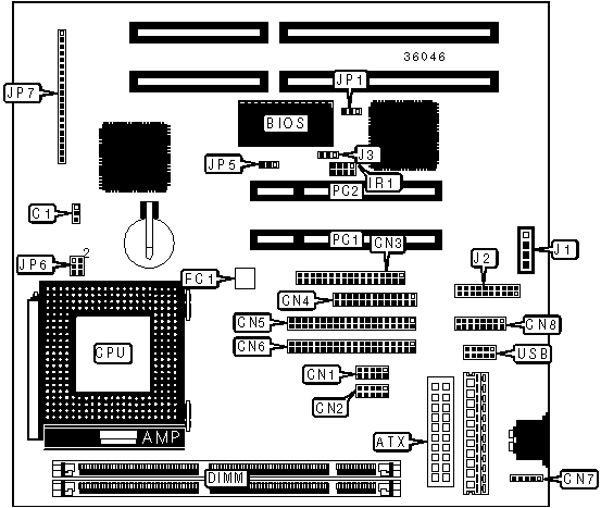
32-bit PCI slots (2), floppy drive interface, game interface, IDE interfaces (2), parallel port, PS/2 mouse interface, serial ports (2), IR connector, USB connector, ATX power connector, audio in – CD-ROM, wake on modem connector |
|
CONNECTIONS | |||
|
Purpose |
Location |
Purpose |
Location |
|
ATX power connector |
ATX |
Audio in – CD-ROM |
J1 |
|
Chassis fan power |
C1 |
Multimedia connector |
J2 |
|
Serial port 2 |
CN1 |
Wake on LAN connector |
J3 |
|
Serial port 1 |
CN2 |
Power LED & keylock |
JP7/pins 1 – 5 |
|
Floppy drive interface |
CN3 |
Speaker |
JP7/pins 7 – 10 |
|
Parallel port |
CN4 |
Reset switch |
JP7/pins 12 & 13 |
|
IDE interface 1 |
CN5 |
IDE interface LED |
JP7/pins 15 & 16 |
|
IDE interface 2 |
CN6 |
Turbo LED |
JP7/pins 18 & 19 |
|
PS/2 mouse interface |
CN7 |
Soft off power supply |
JP7/pins 21 & 22 |
|
Game interface |
CN8 |
32-bit PCI slots |
PC1 – PC2 |
|
IR connector |
IR1 |
USB connector |
USB |
|
USER CONFIGURABLE SETTINGS | |||
|
Function |
Label |
Position | |
|
» |
Factory configured - do not alter |
FC1 |
Unidentified |
|
Flash BIOS voltage select 12v |
JP1 |
Pins 2 & 3 closed | |
|
Flash BIOS voltage select 5v |
JP1 |
Pins 1 & 2 closed | |
|
» |
CMOS memory normal operation |
JP5 |
Pins 1 & 2 closed |
|
CMOS memory clear |
JP5 |
Pins 2 & 3 closed | |
|
DIMM CONFIGURATION | ||
|
Size |
Bank 0 |
Bank 1 |
|
8MB |
(1) 1M x 64 |
None |
|
16MB |
(1) 2M x 64 |
None |
|
16MB |
(1) 1M x 64 |
(1) 1M x 64 |
|
24MB |
(1) 2M x 64 |
(1) 1M x 64 |
|
32MB |
(1) 4M x 64 |
None |
|
32MB |
(1) 2M x 64 |
(1) 2M x 64 |
|
40MB |
(1) 4M x 64 |
(1) 1M x 64 |
|
48MB |
(1) 4M x 64 |
(1) 2M x 64 |
|
64MB |
(1) 8M x 64 |
None |
|
64MB |
(1) 4M x 64 |
(1) 4M x 64 |
|
72MB |
(1) 8M x 64 |
(1) 1M x 64 |
|
80MB |
(1) 8M x 64 |
(1) 2M x 64 |
|
128MB |
(1) 16M x 64 |
None |
|
128MB |
(1) 8M x 64 |
(1) 8M x 64 |
|
136MB |
(1) 16M x 64 |
(1) 1M x 64 |
|
144MB |
(1) 16M x 64 |
(1) 2M x 64 |
|
160MB |
(1) 16M x 64 |
(1) 4M x 64 |
|
192MB |
(1) 16M x 64 |
(1) 8M x 64 |
|
256MB |
(1) 16M x 64 |
(1) 16M x 64 |
|
Note: Board accepts SDRAM memory. | ||
|
CACHE CONFIGURATION |
|
Note: The location of the cache is unidentified. |
|
CPU SPEED SELECTION | |||||
|
CPU speed |
Clock speed |
Multiplier |
JP6/pins 1 & 2 |
JP6/pins 3 & 4 |
JP6/pins 5 & 6 |
|
233MHz |
33MHz |
7x |
Closed |
Open |
Open |
|
266MHz |
33MHz |
8x |
Open |
Open |
Open |
|
300MHz |
33MHz |
9x |
Closed |
Open |
Closed |