CSS LABORATORIES, INC.
MB-5865
|
Processor |
Pentium |
|
Processor Speed |
75/90/100/120/133/150/166/200MHz |
|
Chip Set |
Unidentified |
|
Video Chip Set |
None |
|
Maximum Onboard Memory |
384MB |
|
Maximum Video Memory |
None |
|
Cache |
256/512KB |
|
BIOS |
Unidentified |
|
Dimensions |
330mm x 218mm |
|
I/O Options |
32-bit PCI slots (4), floppy drive interface, IDE interfaces (2), parallel port, PS/2 mouse interface, serial ports (2), cache slot, IR connector, VRM connector, USB connectors (2) |
|
NPU Options |
None |
|
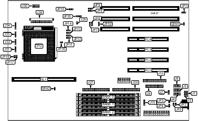
CONNECTIONS | |||
|
Purpose |
Location |
Purpose |
Location |
|
USB connector |
J1 |
VRM connector |
J29 |
|
USB connector |
J3 |
Front panel connector |
J30 |
|
Auxiliary keyboard/mouse connector |
J4 |
IDE interface LED |
J31 |
|
Serial port 1 |
J5 |
Reset switch |
J32/pins 1 & 2 |
|
Serial port 2 |
J6 |
Turbo LED |
J32/pins 3 & 4 |
|
IR connector |
J7 |
Speaker |
J33 |
|
Parallel port |
J9 |
Power LED & keylock |
J34 |
|
Floppy drive interface |
J10 |
32-bit PCI slots |
PC1 – PC4 |
|
External battery |
J15 |
Cache slot |
SL1 |
|
IDE interface 2 |
J20 |
Temperature sensor |
SEN1 |
|
IDE interface 1 |
J27 |
Temperature sensor |
SEN2 |
|
USER CONFIGURABLE SETTINGS | |||
|
Function |
Label |
Position | |
|
» |
Factory configured - do not alter (CMOS password) |
JP2 |
Unidentified |
|
» |
Factory configured - do not alter (CMOS clear) |
JP3 |
Unidentified |
|
» |
Factory configured - do not alter (auxiliary keyboard enabled) |
JP4 |
Unidentified |
|
» |
Factory configured - do not alter (auxiliary keyboard enabled) |
JP5 |
Unidentified |
|
ISA bus clock select /3 |
JP10 |
Pins 1 & 2 closed | |
|
ISA bus clock select /4 |
JP10 |
Pins 2 & 3 closed | |
|
Turbo LED used as turbo LED |
JP15 |
Pins 1 & 2 closed | |
|
Turbo LED used as green PC LED |
JP15 |
Pins 2 & 3 closed | |
|
» |
Next address normal operation |
JP16 |
Closed |
|
Next address not allowed |
JP16 |
Open | |
|
» |
Factory configured - do not alter |
JP35 |
Unidentified |
|
DRAM CONFIGURATION | |||
|
Size |
Bank 0 |
Bank 1 |
Bank 2 |
|
8MB |
(2) 1M x 36 |
None |
None |
|
16MB |
(2) 1M x 36 |
(2) 1M x 36 |
None |
|
16MB |
(2) 2M x 36 |
None |
None |
|
20MB |
(2) 1M x 36 |
(2) 1M x 36 |
(2) 512K x 36 |
|
20MB |
(2) 2M x 36 |
(2) 512K x 36 |
None |
|
24MB |
(2) 2M x 36 |
(2) 1M x 36 |
None |
|
24MB |
(2) 1M x 36 |
(2) 1M x 36 |
(2) 1M x 36 |
|
24MB |
(2) 2M x 36 |
(2) 512K x 36 |
(2) 512K x 36 |
|
28MB |
(2) 2M x 36 |
(2) 1M x 36 |
(2) 512K x 36 |
|
32MB |
(2) 4M x 36 |
None |
None |
|
32MB |
(2) 2M x 36 |
(2) 2M x 36 |
None |
|
40MB |
(2) 4M x 36 |
(2) 1M x 36 |
None |
|
40MB |
(2) 4M x 36 |
(2) 512K x 36 |
(2) 512K x 36 |
|
44MB |
(2) 4M x 36 |
(2) 1M x 36 |
(2) 512K x 36 |
|
DRAM CONFIGURATION (CON’T) | |||
|
Size |
Bank 0 |
Bank 1 |
Bank 2 |
|
48MB |
(2) 4M x 36 |
(2) 2M x 36 |
None |
|
48MB |
(2) 4M x 36 |
(2) 1M x 36 |
(2) 1M x 36 |
|
52MB |
(2) 4M x 36 |
(2) 2M x 36 |
(2) 512K x 36 |
|
56MB |
(2) 4M x 36 |
(2) 2M x 36 |
(2) 1M x 36 |
|
64MB |
(2) 8M x 36 |
None |
None |
|
64MB |
(2) 4M x 36 |
(2) 4M x 36 |
None |
|
68MB |
(2) 8M x 36 |
(2) 512K x 36 |
None |
|
68MB |
(2) 4M x 36 |
(2) 4M x 36 |
(2) 512K x 36 |
|
72MB |
(2) 8M x 36 |
(2) 512K x 36 |
(2) 512K x 36 |
|
76MB |
(2) 8M x 36 |
(2) 512K x 36 |
(2) 1M x 36 |
|
80MB |
(2) 8M x 36 |
(2) 2M x 36 |
None |
|
80MB |
(2) 8M x 36 |
(2) 1M x 36 |
(2) 1M x 36 |
|
84MB |
(2) 8M x 36 |
(2) 2M x 36 |
(2) 512K x 36 |
|
88MB |
(2) 8M x 36 |
(2) 2M x 36 |
(2) 1M x 36 |
|
96MB |
(2) 8M x 36 |
(2) 4M x 36 |
None |
|
96MB |
(2) 4M x 36 |
(2) 4M x 36 |
(2) 4M x 36 |
|
96MB |
(2) 8M x 36 |
(2) 2M x 36 |
(2) 2M x 36 |
|
100MB |
(2) 8M x 36 |
(2) 4M x 36 |
(2) 512K x 36 |
|
104MB |
(2) 8M x 36 |
(2) 4M x 36 |
(2) 1M x 36 |
|
112MB |
(2) 8M x 36 |
(2) 4M x 36 |
(2) 2M x 36 |
|
128MB |
(2) 8M x 36 |
(2) 4M x 36 |
(2) 4M x 36 |
|
128MB |
(2) 16M x 36 |
None |
None |
|
128MB |
(2) 8M x 36 |
(2) 8M x 36 |
None |
|
132MB |
(2) 8M x 36 |
(2) 8M x 36 |
(2) 512K x 36 |
|
132MB |
(2) 16M x 36 |
(2) 512K x 36 |
None |
|
136MB |
(2) 8M x 36 |
(2) 8M x 36 |
(2) 1M x 36 |
|
136MB |
(2) 16M x 36 |
(2) 1M x 36 |
None |
|
140MB |
(2) 16M x 36 |
(2) 1M x 36 |
(2) 512K x 36 |
|
144MB |
(2) 16M x 36 |
(2) 2M x 36 |
None |
|
144MB |
(2) 16M x 36 |
(2) 1M x 36 |
(2) 1M x 36 |
|
148MB |
(2) 16M x 36 |
(2) 2M x 36 |
(2) 512K x 36 |
|
152MB |
(2) 16M x 36 |
(2) 2M x 36 |
(2) 1M x 36 |
|
160MB |
(2) 16M x 36 |
(2) 4M x 36 |
None |
|
160MB |
(2) 16M x 36 |
(2) 2M x 36 |
(2) 2M x 36 |
|
164MB |
(2) 16M x 36 |
(2) 4M x 36 |
(2) 512K x 36 |
|
168MB |
(2) 16M x 36 |
(2) 4M x 36 |
(2) 1M x 36 |
|
176MB |
(2) 16M x 36 |
(2) 4M x 36 |
(2) 2M x 36 |
|
192MB |
(2) 16M x 36 |
(2) 8M x 36 |
None |
|
192MB |
(2) 16M x 36 |
(2) 4M x 36 |
(2) 4M x 36 |
|
196MB |
(2) 16M x 36 |
(2) 8M x 36 |
(2) 512K x 36 |
|
200MB |
(2) 16M x 36 |
(2) 8M x 36 |
(2) 1M x 36 |
|
208MB |
(2) 16M x 36 |
(2) 8M x 36 |
(2) 2M x 36 |
|
DRAM CONFIGURATION (CON’T) | |||
|
Size |
Bank 0 |
Bank 1 |
Bank 2 |
|
224MB |
(2) 16M x 36 |
(2) 8M x 36 |
(2) 4M x 36 |
|
256MB |
(2) 16M x 36 |
(2) 16M x 36 |
None |
|
256MB |
(2) 16M x 36 |
(2) 8M x 36 |
(2) 8M x 36 |
|
260MB |
(2) 16M x 36 |
(2) 16M x 36 |
(2) 512K x 36 |
|
264MB |
(2) 16M x 36 |
(2) 16M x 36 |
(2) 1M x 36 |
|
272MB |
(2) 16M x 36 |
(2) 16M x 36 |
(2) 2M x 36 |
|
288MB |
(2) 16M x 36 |
(2) 16M x 36 |
(2) 4M x 36 |
|
320MB |
(2) 16M x 36 |
(2) 16M x 36 |
(2) 8M x 36 |
|
384MB |
(2) 16M x 36 |
(2) 16M x 36 |
(2) 16M x 36 |
|
Note: Board also accepts x 32 SIMMs. | |||
|
DRAM REFRESH RATE CONFIGURATION | |
|
Refresh rate |
J28 |
|
60MHz |
Closed |
|
66MHz |
Open |
|
CACHE CONFIGURATION | |
|
Size |
SL1 |
|
256KB |
256KB module installed |
|
512KB |
512KB module installed |
|
CACHE JUMPER CONFIGURATION | ||
|
Size |
JP13 |
JP14 |
|
None |
Pins 1 & 2 closed |
Pins 1 & 2 closed |
|
256KB |
Pins 2 & 3 closed |
Pins 1 & 2 closed |
|
512KB |
Pins 1 & 2 closed |
Pins 2 & 3 closed |
|
CACHE TYPE CONFIGURATION | ||
|
Type |
JP11 |
JP12 |
|
1-bank pipeline burst |
Pins 1 & 2 closed |
Pins 1 & 2 closed |
|
2-bank pipeline burst |
Pins 2 & 3 closed |
Pins 2 & 3 closed |
|
CPU SPEED SELECTION | ||||||
|
CPU speed |
Clock speed |
Multiplier |
JP6 |
JP7 |
JP17 |
JP18 |
|
75MHz |
50MHz |
1.5x |
2 & 3 |
2 & 3 |
Open |
Open |
|
90MHz |
60MHz |
1.5x |
2 & 3 |
1 & 2 |
Open |
Open |
|
100MHz |
66MHz |
1.5x |
1 & 2 |
2 & 3 |
Open |
Open |
|
120MHz |
60MHz |
2x |
2 & 3 |
1 & 2 |
Open |
Closed |
|
133MHz |
66MHz |
2x |
1 & 2 |
2 & 3 |
Open |
Closed |
|
150MHz |
60MHz |
2.5x |
2 & 3 |
1 & 2 |
Closed |
Closed |
|
166MHz |
66MHz |
2.5x |
1 & 2 |
2 & 3 |
Closed |
Closed |
|
200MHz |
66MHz |
3x |
1 & 2 |
2 & 3 |
Closed |
Open |
|
Note: Pins designated should be in the closed position. | ||||||
|
FLASH BIOS SELECTION | |||
|
Setting |
JP1 |
JP8 |
JP9 |
|
Normal operation |
Pins 1 & 2 closed |
Pins 1 & 2 closed |
Pins 1 & 2 closed |
|
Programming mode |
Pins 1 & 2 closed |
Pins 2 & 3 closed |
Pins 2 & 3 closed |