DATAVAN INTERNATIONAL CORPORATION
DTV-05C
|
Processor |
80486SX/80486DX/CX486DX2/80486DX2/CX486DX4/ AM486DX4(V8B)/AM486DX4(V8T)/80486DX4(WB)/80486DX4(WT)/ AM5X86/CX5X86 |
|
Processor Speed |
25/33/40/50(internal)/50/66(internal)/80(internal)/100(internal)/ 120(internal)/133(internal)MHz |
|
Chip Set |
ALI |
|
Video Chip Set |
Cirrus Logic |
|
Maximum Onboard Memory |
32MB |
|
Maximum Video Memory |
Unidentified |
|
Cache |
64/128/256KB |
|
BIOS |
AMI |
|
Dimensions |
270mm x 150mm |
|
I/O Options |
Floppy drive interface, IDE interface, parallel port, serial ports (2), VGA feature connector, VGA port |
|
NPU Options |
None |
|
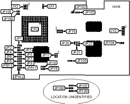
CONNECTIONS | |||
|
Purpose |
Location |
Purpose |
Location |
|
Chassis fan power |
CN100 |
VGA feature connector |
P1 |
|
Power LED |
JP13 |
VGA port |
P2 |
|
Speaker |
JP14 |
IDE interface |
PV1 |
|
Turbo LED |
JP15 |
Floppy drive interface |
PV2 |
|
Reset switch |
JP24 |
Serial port 1 |
PV4 |
|
Chassis fan power |
JP101 |
Serial port 2 |
PV5 |
|
IDE interface LED |
JV1 |
Parallel port |
PV6 |
|
Note: The locations of all connectors are unidentified. | |||
|
USER CONFIGURABLE SETTINGS | |||
|
Function |
Label |
Position | |
|
» |
Factory configured – do not alter |
JP2 |
Closed |
|
» |
Factory configured – do not alter |
JP3 |
Closed |
|
» |
Factory configured – do not alter |
JP4 |
Pins 2 & 3 closed |
|
» |
Factory configured – do not alter |
JP5 |
Pins 2 & 3 closed |
|
» |
Factory configured – do not alter |
JP6 |
Pins 1 & 2 closed |
|
» |
Factory configured – do not alter |
JP7 |
Pins 1 & 2 closed |
|
» |
Factory configured – do not alter |
JP9 |
Pins 2 & 3 closed |
|
» |
Factory configured – do not alter |
JP18 |
Pins 2 & 3 closed |
|
» |
Factory configured – do not alter |
JP19 |
Pins 2 & 3 closed |
|
» |
On board video enabled |
JP100 |
Pins 1 & 2 closed |
|
On board video disabled |
JP100 |
Pins 2 & 3 closed | |
|
» |
CMOS memory normal operation |
JP105 |
Open |
|
CMOS memory clear |
JP105 |
Closed | |
|
» |
Factory configured – do not alter |
JP106 |
Open |
|
» |
Factory configured – do not alter |
JP107 |
Pins 1 & 2 closed |
|
» |
Factory configured – do not alter |
JP108 |
Pins 1 & 2 closed |
|
» |
Factory configured – do not alter |
JP109 |
Pins 1 & 2 closed |
|
» |
Factory configured – do not alter |
JPA12 |
Closed |
|
» |
Floppy drive interface enabled |
JV2/pins 5 & 6 |
Closed |
|
Floppy drive interface disabled |
JV2/pins 5 & 6 |
Open | |
|
» |
IDE interface enabled |
JV2/pins 7 & 8 |
Closed |
|
IDE interface disabled |
JV2/pins 7 & 8 |
Open | |
|
» |
Serial port 1 enabled |
JV2/pins 9 & 10 |
Closed |
|
Serial port 1 disabled |
JV2/pins 9 & 10 |
Open | |
|
» |
Serial port 2 enabled |
JV2/pins 11 & 12 |
Closed |
|
Serial port 2 disabled |
JV2/pins 11 & 12 |
Open | |
|
DRAM CONFIGURATION | ||
|
Size |
Bank 0 |
Bank 1 |
|
2MB |
(1) 256K x 36 |
(1) 256K x 36 |
|
4MB |
(1) 1M x 36 |
None |
|
8MB |
(1) 1M x 36 |
(1) 1M x 36 |
|
8MB |
(1) 2M x 36 |
None |
|
16MB |
(1) 4M x 36 |
None |
|
32MB |
(1) 4M x 36 |
(1) 4M x 36 |
|
Note: The location of banks 0 & 1 is unidentified. | ||
|
CACHE CONFIGURATION |
|
Note: Board accepts 64KB/128KB/256KB cache. The location and chip sizes are unidentified. |
|
CACHE JUMPER CONFIGURATION | ||||
|
Size |
JP17 |
JP20 |
JP21 |
JP23 |
|
64KB |
1 & 2 |
Open |
1 & 2 |
1 & 2 |
|
128KB |
1 & 2, 3 & 4 |
Closed |
2 & 3 |
1 & 2 |
|
256KB |
1 & 2, 3 & 4, 5 & 6 |
Closed |
1 & 2 |
1 & 2 |
|
Note: Pins designated should be in the closed position. | ||||
|
CPU SPEED SELECTION | |
|
Speed |
JP16 |
|
25MHz |
Pins 1 & 2, 5 & 6 closed |
|
33MHz |
Pins 1 & 2, 3 & 4 closed |
|
40MHz |
Pins 3 & 4, 5 & 6, 7 & 8 closed |
|
50iMHz |
Pins 1 & 2, 5 & 6 closed |
|
50MHz |
Pins 1 & 2, 5 & 6, 7 & 8 closed |
|
66iMHz |
Pins 1 & 2, 3 & 4, 7 & 8 closed |
|
80iMHz |
Pins 5 & 6, 7 & 8 closed |
|
100iMHz |
Pins 3 & 4, 7 & 8 closed |
|
120iMHz |
Pins 3 & 4, 5 & 6, 7 & 8 closed |
|
133iMHz |
Pins 1 & 2, 3 & 4 closed |
|
CPU TYPE SELECTION | ||||
|
Type |
JP1 |
JP8 |
JPB13 |
JPR17 |
|
80486SX |
Open |
Pins 1 & 2 closed |
Open |
Open |
|
80486DX |
Open |
Pins 1 & 2 closed |
Open |
Open |
|
CX486DX2 |
Closed |
Pins 2 & 3 closed |
Open |
Pins 1 & 2 closed |
|
80486DX2 |
Open |
Pins 1 & 2 closed |
Open |
Open |
|
CX486DX4 |
Closed |
Pins 2 & 3 closed |
Open |
Pins 1 & 2 closed |
|
AM486DX4 (V8B) |
Open |
Pins 2 & 3 closed |
Open |
Open |
|
AM486DX4 (V8T) |
Open |
Pins 1 & 2 closed |
Pins 2 & 3 closed |
Open |
|
80486DX4 (WB) |
Open |
Pins 2 & 3 closed |
Open |
Open |
|
80486DX4 (WT) |
Open |
Pins 1 & 2 closed |
Open |
Open |
|
CX5X86 |
Open |
Pins 2 & 3 closed |
Open |
Open |
|
AM5X86 |
Open |
Pins 2 & 3 closed |
Open |
Pins 2 & 3 closed |
|
CPU VOLTAGE SELECTION | ||
|
Voltage |
JX1 |
JX2 |
|
3.3v |
Pins 1 & 2 closed |
Pins 4 & 7, 5 & 8, 6 & 9 closed |
|
3.45v |
Pins 2 & 3 closed |
Pins 4 & 7, 5 & 8, 6 & 9 closed |
|
5v |
N/A |
Pins 1 & 4, 2 & 5, 3 & 6 closed |
|
PARALLEL PORT ADDRESS SELECTION | ||
|
Setting |
JV2 | |
| » |
378h |
Pins 3 & 4 closed |
|
278h |
Pins 1 & 2 closed | |
|
3BCh |
Pins 1 & 2, 3 & 4 closed | |
|
Disabled |
Open | |
|
SERIAL PORT ADDRESS SELECTION | ||
|
Setting |
JP102 | |
| » |
COM1 (3F8h)/COM2 (2F8h) |
Open |
|
COM3 (3E8h)/COM4 (2E8h) |
Closed | |
|
SERIAL PORT SELECTION | ||
|
Setting |
JP103 |
JP104 |
|
Normal pin out |
Pins 2 & 3 closed |
Pins 2 & 3 closed |
|
9 th pin out with+5v for CCD |
Pins 1 & 2 closed |
Pins 1 & 2 closed |