AT & T
MODEL 6386E/33 WGS (FM-0589-10)
MODEL 6386E/33S WGS (FM-0589-11)
|
Processor |
80386 |
|
Processor Speed |
33MHz |
|
Chip Set |
Unidentified |
|
Video Chip Set |
None |
|
Maximum Onboard Memory |
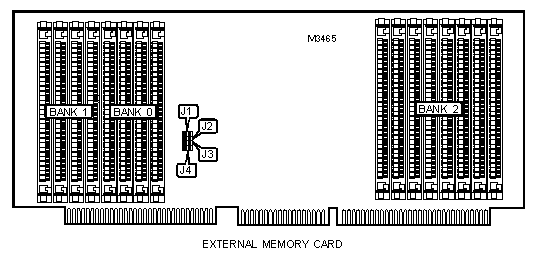
8MB (16MB on external memory card) |
|
Maximum Video Memory |
None |
|
Cache |
64KB |
|
BIOS |
Unidentified |
|
Dimensions |
355mm x 304mm |
|
I/O Options |
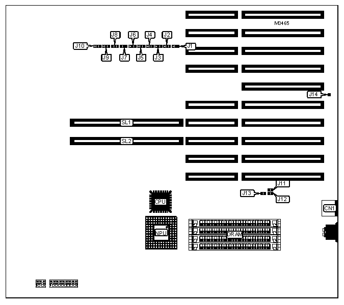
External memory cards (2), PS/2 mouse port, parallel port, serial ports (2) |
|
NPU Options |
80387/3167 |
|
CONNECTIONS | |||
|
Purpose |
Location |
Purpose |
Location |
|
PS/2 mouse port |
CN1 |
External memory cards |
SL1 & SL2 |
|
Remote reset switch |
J14 | ||
|
Note: Mainboard has 2 serial ports and 1 parallel port. The location is unidentified. | |||
|
USER CONFIGURABLE SETTINGS | |||
|
Function |
Label |
Position | |
|
» |
Password normal operation |
J1 |
Pins 2 & 3 closed |
|
Password clear |
J1 |
Pins 1 & 2 closed | |
|
Monitor type select color |
J6 |
Pins 1 & 2 closed | |
|
Monitor type select monochrome |
J6 |
Pins 2 & 3 closed | |
|
Jumper information unavailable |
J7 |
Unidentified | |
|
Jumper information unavailable |
J8 |
Unidentified | |
|
Printer acknowledge signal edge leading edge |
J9 |
Pins 2 & 3 closed | |
|
Printer acknowledge signal edge trailing edge |
J9 |
Pins 1 & 2 closed | |
|
BIOS type select 64KB |
J10 |
Pins 2 & 3 closed | |
|
BIOS type select 128KB |
J10 |
Pins 1 & 2 closed | |
|
DRAM CONFIGURATION | ||
|
Size |
Bank 0 |
Bank 1 |
|
4MB |
(2) 1M x 9 |
(2) 1M x 9 |
|
8MB |
(2) 4M x 9 |
None |
|
Note: The location of banks 0 & 1 are unidentified. | ||
|
DRAM JUMPER CONFIGURATION | |||
|
Size |
J11 |
J12 |
J13 |
|
4MB |
Closed |
Open |
Closed |
|
8MB |
Closed |
Closed |
Open |
|
CACHE CONFIGURATION |
|
Note: The location of the 64KB cache is unidentified. |
|
PARALLEL PORT ADDRESS SELECTION | ||
|
Setting |
J2 |
J3 |
|
LPT1 (378h) |
Pins 2 & 3 closed |
Pins 1 & 2 closed |
|
LPT2 (278h) |
Pins 1 & 2 closed |
Pins 2 & 3 closed |
|
Disabled |
Pins 1 & 2 closed |
Pins 1 & 2 closed |
|
SERIAL PORT 1 ADDRESS SELECTION | |
|
Setting |
J4 |
|
COM1 (3F8h) |
Pins 2 & 3 closed |
|
Disabled |
Pins 1 & 2 closed |
|
SERIAL PORT 2 ADDRESS SELECTION | |
|
Setting |
J5 |
|
COM2 (2F8h) |
Pins 2 & 3 closed |
|
Disabled |
Pins 1 & 2 closed |
|
DRAM CONFIGURATION | |||
|
Size |
Bank 0 |
Bank 1 |
Bank 2 |
|
4MB |
(4) 1M x 9 |
None |
None |
|
8MB |
(4) 1M x 9 |
(4) 1M x 9 |
None |
|
16MB |
(4) 1M x 9 |
(4) 1M x 9 |
(8) 1M x 9 |
|
DRAM JUMPER CONFIGURATION | ||||
|
Size |
J1 |
J2 |
J3 |
J4 |
|
4MB |
Closed |
Open |
Open |
Closed |
|
8MB |
Open |
Closed |
Closed |
Open |
|
16MB |
Closed |
Closed |
Open |
Open |
|
MISCELLANEOUS TECHINCAL NOTE |
|
Don’t remove jumper from pins E52 and E53. The location of these pins are unidentified. |