TYAN COMPUTER CORPORATION
S1344
|
| |
|
Data bus: |
32-bit, VL-bus |
|
Size: |
Three/quarter-length, half-height card |
|
Hard drive supported: |
Four IDE (AT) Interface drives |
|
Floppy drives supported: |
Four 360KB, 720KB, 1.2MB, or 1.44MB drives |
|
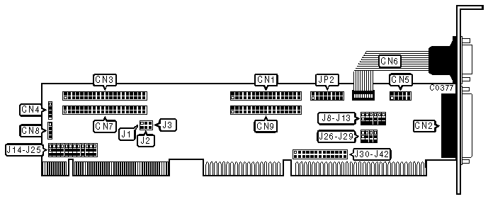
CONNECTIONS | |
|
Function |
Location |
|
34-pin control cable connector - floppy drive 1 |
CN1 |
|
25-pin parallel port (LPT1/2/3) - external |
CN2 |
|
40-pin IDE(AT) Interface (IDE-0) |
CN3 |
|
4-pin connector - Drive active (IDE-0) |
CN4 |
|
10-pin serial port (COM1/2/4) - internal |
CN5 |
|
10-pin serial port (COM1/2/3) - external |
CN6 |
|
40-pin IDE(AT) Interface (IDE-1) |
CN7 |
|
4-pin connector - Drive active (IDE-1) |
CN8 |
|
34-pin control cable connector - floppy drive 2 |
CN9 |
|
15-pin game port - internal |
JP2 |
|
USER CONFIGURABLE SETTINGS | |||
|
Function |
Location |
Setting | |
| » |
I/O Channel Ready signal disabled |
J1 |
open |
|
I/O Channel Ready signal enabled |
J1 |
closed | |
| » |
Floppy drive compatible mode |
J7 |
pins 2 & 3 closed |
|
Floppy drive enhanced mode |
J7 |
pins 1 & 2 closed | |
| » |
Floppy drive enabled |
J8 |
pins 2 & 3 closed |
|
Floppy drive disabled |
J8 |
pins 1 & 2 closed | |
| » |
Uses VL Ready |
J14 |
pins 2 & 3 closed |
|
Use CPU Ready |
J14 |
pins 1 & 2 closed | |
|
USER CONFIGURABLE SETTINGS | |||
|
Function |
Location |
Setting | |
| » |
Hard drive enabled |
J15 |
pins 2 & 3 closed |
|
Hard drive disabled |
J15 |
pins 1 & 2 closed | |
| » |
Floppy drive port address is 3F0-3F7h |
J26 |
pins 2 & 3 closed |
|
Floppy drive port address is 370-377h |
J26 |
pins 1 & 2 closed | |
| » |
Floppy drive interrupt is IRQ6 |
J35 |
closed |
|
Floppy drive interrupt is disabled |
J35 |
open | |
| » |
Game Port enabled |
J42 |
closed |
|
Game Port disabled |
J42 |
open | |
|
HARD DRIVE INTERRUPT REQUEST | |||
|
Function |
J2 |
J3 | |
| » |
IRQ14 for IDE-0 (CN3) |
open |
closed |
|
IRQ15 for IDE-1 (CN7) |
closed |
open | |
|
IRQ14 for IDE-0, IRQ 15 for IDE-1 |
closed |
closed | |
|
IDE Interrupt disabled |
open |
open | |
|
PARALLEL PORT (CN2) CONFIGURATION | |||
|
LPT |
J9 |
J27 | |
| » |
LPT1 |
pins 2 & 3 closed |
pins 2 & 3 closed |
|
LPT2 |
pins 2 & 3 closed |
pins 1 & 2 closed | |
|
LPT3 |
pins 1 & 2 closed |
pins 1 & 2 closed | |
|
Disabled |
pins 1 & 2 closed |
pins 2 & 3 closed | |
|
SERIAL PORT 1 (CN6) CONFIGURATION | |||
|
COM |
J10 |
J11 | |
| » |
COM1 |
pins 2 & 3 closed |
pins 2 & 3 closed |
|
COM2 |
pins 2 & 3 closed |
pins 1 & 2 closed | |
|
COM3 |
pins 1 & 2 closed |
pins 2 & 3 closed | |
|
Disabled |
pins 1 & 2 closed |
pins 1 & 2 closed | |
|
SERIAL PORT 2 (CN5) CONFIGURATION | |||
|
COM |
J12 |
J13 | |
|
COM1 |
pins 2 & 3 closed |
pins 1 & 2 closed | |
| » |
COM2 |
pins 2 & 3 closed |
pins 2 & 3 closed |
|
COM4 |
pins 1 & 2 closed |
pins 2 & 3 closed | |
|
Disabled |
pins 1 & 2 closed |
pins 1 & 2 closed | |
|
HARD DRIVE ADDRESS | ||||
|
IDE 0 Address |
IDE 1 Address |
J18 |
J19 | |
|
1F0-1F7h |
1F0-1F7h |
pins 1 & 2 closed |
pins 1 & 2 closed | |
|
1F0-1F7h |
170-177h |
pins 1 & 2 closed |
pins 2 & 3 closed | |
|
170-177h |
disabled |
pins 2 & 3 closed |
pins 1 & 2 closed | |
| » |
1F0-1F7h |
disabled |
pins 2 & 3 closed |
pins 2 & 3 closed |
|
IDE 0 (CN3) WAIT STATE | ||||
|
Speed |
J20 |
J21 |
J22 | |
|
16MHz VL Bus Clock |
Pins 1 & 2 closed |
Pins 1 & 2 closed |
Pins 1 & 2 closed | |
|
20 or 25MHz VL Bus Clock |
Pins 1 & 2 closed |
Pins 1 & 2 closed |
Pins 2 & 3 closed | |
|
25 or 33MHz VL Bus Clock |
Pins 1 & 2 closed |
Pins 2 & 3 closed |
Pins 1 & 2 closed | |
|
33MHz VL Bus Clock |
Pins 1 & 2 closed |
Pins 2 & 3 closed |
Pins 2 & 3 closed | |
|
40MHz VL Bus Clock |
Pins 2 & 3 closed |
Pins 1 & 2 closed |
Pins 1 & 2 closed | |
|
50MHz VL Bus Clock |
Pins 2 & 3 closed |
Pins 1 & 2 closed |
Pins 2 & 3 closed | |
|
50MHz VL Bus Clock |
Pins 2 & 3 closed |
Pins 2 & 3 closed |
Pins 1 & 2 closed | |
| » |
50MHz VL Bus Clock |
Pins 2 & 3 closed |
Pins 2 & 3 closed |
Pins 2 & 3 closed |
|
IDE 1 (CN7) WAIT STATE | ||||
|
Speed |
J23 |
J24 |
J25 | |
|
16MHz VL Bus Clock |
Pins 1 & 2 closed |
Pins 1 & 2 closed |
Pins 1 & 2 closed | |
|
20 or 25MHz VL Bus Clock |
Pins 1 & 2 closed |
Pins 1 & 2 closed |
Pins 2 & 3 closed | |
|
25 or 33MHz VL Bus Clock |
Pins 1 & 2 closed |
Pins 2 & 3 closed |
Pins 1 & 2 closed | |
|
33MHz VL Bus Clock |
Pins 1 & 2 closed |
Pins 2 & 3 closed |
Pins 2 & 3 closed | |
|
40MHz VL Bus Clock |
Pins 2 & 3 closed |
Pins 1 & 2 closed |
Pins 1 & 2 closed | |
|
50MHz VL Bus Clock |
Pins 2 & 3 closed |
Pins 1 & 2 closed |
Pins 2 & 3 closed | |
|
50MHz VL Bus Clock |
Pins 2 & 3 closed |
Pins 2 & 3 closed |
Pins 1 & 2 closed | |
| » |
50MHz VL Bus Clock |
Pins 2 & 3 closed |
Pins 2 & 3 closed |
Pins 2 & 3 closed |
|
SERIAL PORT 2 (CN5) INTERRUPT REQUEST | ||||
|
IRQ |
J30 |
J31 |
J32 | |
| » |
3 |
open |
closed |
open |
|
4 |
open |
bottom (pin 2) of J31 & bottom (pin2) of J32 closed | ||
|
5 |
closed |
open |
open | |
|
SERIAL PORT 1 (CN6) INTERRUPT REQUEST | ||||
|
IRQ |
J31 |
J32 |
J33 | |
| » |
4 |
open |
closed |
open |
|
5 |
open |
open |
closed | |
|
3 |
top (pin 1) of J31 & top (pin 1) of J32 closed |
open | ||
|
PARALLEL PORT (CN2) INTERRUPT REQUEST | |||
|
IRQ |
J34 |
J36 | |
| » |
Parallel port interrupt is IRQ7 |
open |
closed |
|
Parallel port interrupt is IRQ5 |
closed |
open | |
|
MISCELLANEOUS TECHNICAL NOTES |
|
J16, J17, J28, J29, J37, J38, J39, J40, and J41 are reserved with all pins open - do not alter. |